Electron Microscopy

Scanning Electron Microscopy - Theory and Instrumentation

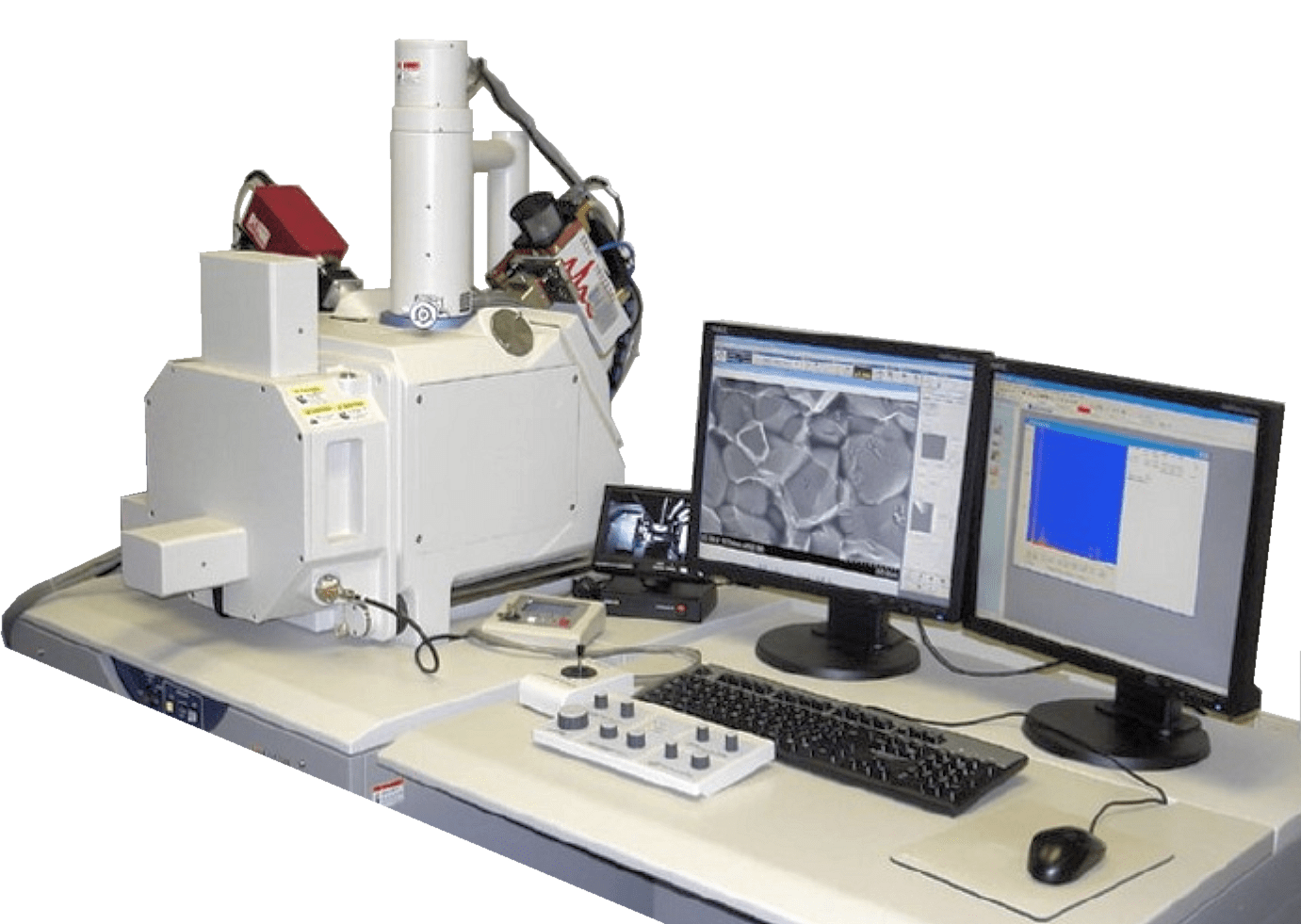
A scanning electron microscope (SEM) is a type of electron microscope that produces images of a sample by scanning the surface with a focused beam of electrons. The electrons interact with atoms in the sample, producing various signals that contain information about the surface topography and composition of the sample. The electron beam is scanned in a raster scan pattern, and the position of the beam is combined with the intensity of the detected signal to produce an image. In the most common SEM mode, secondary electrons emitted by atoms excited by the electron beam are detected using a secondary electron detector (Everhart-Thornley detector). The number of secondary electrons that can be detected, and thus the signal intensity, depends, among other things, on specimen topography. SEM can achieve resolution better than 1 nanometer.

Specimens are observed in high vacuum in conventional SEM, or in low vacuum or wet conditions in variable pressure or environmental SEM, and at a wide range of cryogenic or elevated temperatures with specialized instruments.[1]

Basic principles

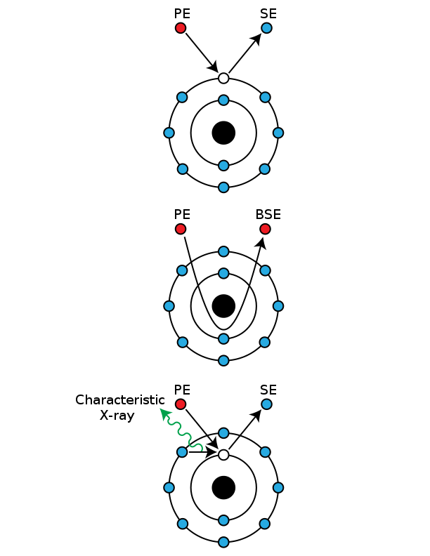
The signals used by a scanning electron microscope to produce an image result from interactions of the electron beam with atoms at various depths within the sample. Various types of signals are produced including secondary electrons (SE), reflected or back-scattered electrons (BSE), characteristic X-rays (EDS) and light (cathodoluminescence) (CL), absorbed current (specimen current) and transmitted electrons.

Secondary electron (SE) detectors are standard equipment in all SEMs, but it is rare for a single machine to have detectors for all other possible signals.

Secondary Electrons (SE)
Secondary electrons have very low energies on the order of 50 eV, which limits their mean free path in solid matter. Consequently, SEs can only escape from the top few nanometers of the surface of a sample. The signal from secondary electrons tends to be highly localized at the point of impact of the primary electron beam, making it possible to collect images of the sample surface with a resolution of below 1 nm.

Backscattered Electrons (BSE)
Back-scattered electrons (BSE) are beam electrons that are reflected from the sample by elastic scattering. They emerge from deeper locations within the specimen and, consequently, the resolution of BSE images is less than SE images. However, BSE are often used in analytical SEM, along with the spectra made from the characteristic X-rays, because the intensity of the BSE signal is strongly related to the atomic number (Z) of the specimen. BSE images can provide information about the distribution, but not the identity, of different elements in the sample.

Energy Dispersive Spectrometry (EDS or EDX)
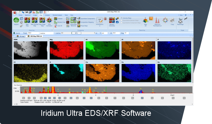
Characteristic X-rays are emitted when the electron beam removes an inner shell electron from the sample, causing a higher-energy electron to fill the shell and release energy. The energy or wavelength of these characteristic X-rays can be measured by energy-dispersive X-ray spectroscopy and used to identify and measure the abundance of elements in the sample and map their distribution.

X-ray Fluorescence (SEM-XRF)
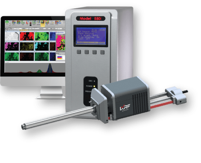
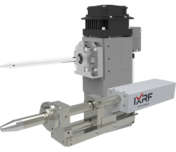
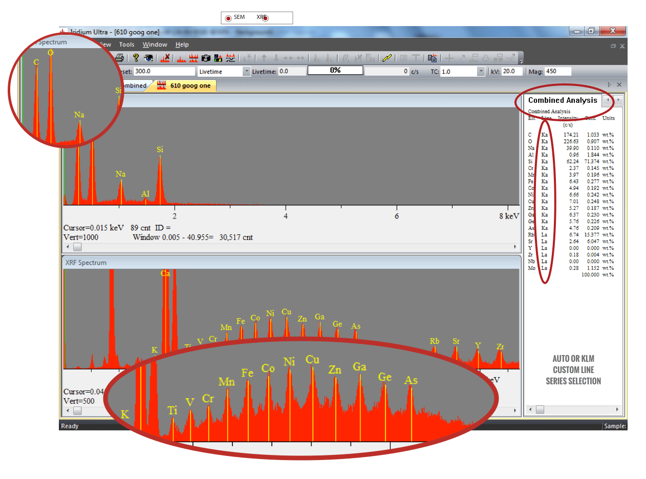
The technological progress in the fields of small-spot low-power X-ray tubes and associated polycapillary X-ray optics has enabled the development of compact micro-focus X-ray sources that can be attached onto a SEM-EDS (scanning electron microscope with energy dispersive X-ray spectrometer) system. As such, micro-spot X-ray fluorescence (μXRF, microEDXRF) can be performed with an SEM so that the analytical capabilities of SEM are considerably extended. Implementation of SEM-XRF is especially attractive due to the possibility of using many existing features offered on existing SEM-EDS systems (e.g. acquisition and identification of the X-ray fluorescence spectra). For example, sample stage control can be used for carrying out X-ray fluorescence (elemental analysis) spectral maps in the manner that is well known in SEM-EDS. By combining the analytical information obtained from the X-ray spectra excited with electrons and with X-ray photons respectively, trace elements of low and high atomic numbers may be quantified, albeit with different spatial resolutions.*

Magnification & Depth of Field
Due to the very narrow electron beam, SEM micrographs have a large depth of field yielding a characteristic three-dimensional appearance useful for understanding the surface structure of a sample. A wide range of magnifications is possible, from about 10 times (about equivalent to that of a powerful hand-lens) to more than 500,000 times, about 250 times the magnification limit of the best light microscopes.

Sample preparation

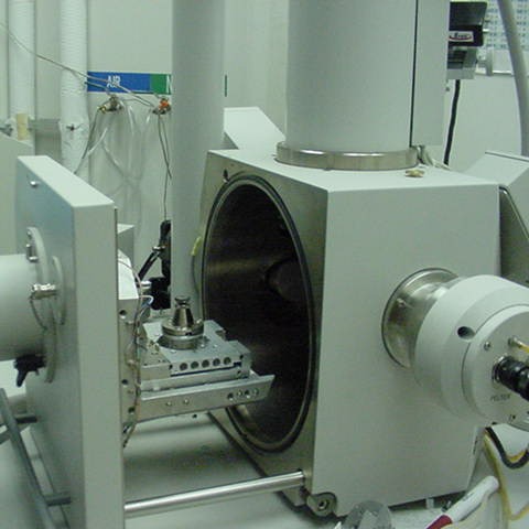
SEM samples have to be small enough to fit on the specimen stage, and may need special preparation to increase their electrical conductivity and to stabilize them, so that they can withstand the high vacuum conditions and the high energy beam of electrons. Samples are generally mounted rigidly on a specimen holder or stub using a conductive adhesive. SEM is used extensively for defect analysis of semiconductor wafers, and manufacturers make instruments that can examine any part of a 300 mm semiconductor wafer. Many instruments have chambers that can tilt an object of that size to 45° and provide continuous 360° rotation.

Nonconductive specimens collect charge when scanned by the electron beam, and especially in secondary electron imaging mode, this causes scanning faults and other image artifacts. For conventional imaging in the SEM, specimens must be electrically conductive, at least at the surface, and electrically grounded to prevent the accumulation of electrostatic charge. Metal objects require little special preparation for SEM except for cleaning and conductively mounting to a specimen stub. Non-conducting materials are usually coated with an ultrathin coating of electrically conducting material, deposited on the sample either by low-vacuum sputter coating or by high-vacuum evaporation. Conductive materials in current use for specimen coating include gold, gold/palladium alloy, platinum, iridium, tungsten, chromium, osmium,[13] and graphite. Coating with heavy metals may increase signal/noise ratio for samples of low atomic number (Z). The improvement arises because secondary electron emission for high-Z materials is enhanced.

Nonconducting specimens may be imaged without coating using an environmental SEM (ESEM) or low-voltage mode of SEM operation.[17] In ESEM instruments the specimen is placed in a relatively high-pressure chamber and the electron optical column is differentially pumped to keep vacuum adequately low at the electron gun. The high-pressure region around the sample in the ESEM neutralizes charge and provides an amplification of the secondary electron signal. Low-voltage SEM is typically conducted in an instrument with a field emission guns (FEG) which is capable of producing high primary electron brightness and small spot size even at low accelerating potentials. To prevent charging of non-conductive specimens, operating conditions must be adjusted such that the incoming beam current is equal to sum of outgoing secondary and backscattered electron currents, a condition that is most often met at accelerating voltages of 0.3–4 kV.

Embedding in a resin with further polishing to a mirror-like finish can be used for both biological and materials specimens when imaging in backscattered electrons or when doing quantitative X-ray microanalysis.

Scanning process

In a typical SEM, an electron beam is thermionically emitted from an electron gun fitted with a tungsten filament cathode. Tungsten is normally used in thermionic electron guns because it has the highest melting point and lowest vapor pressure of all metals, thereby allowing it to be electrically heated for electron emission, and because of its low cost. Other types of electron emitters include lanthanum hexaboride (LaB6) cathodes, which can be used in a standard tungsten filament SEM if the vacuum system is upgraded or field emission guns (FEG), which may be of the cold-cathode type using tungsten single crystal emitters or the thermally assisted Schottky type, that use emitters of zirconium oxide.

The electron beam, which typically has an energy ranging from 0.2 keV to 40 keV, is focused by one or two condenser lenses to a spot about 0.4 nm to 5 nm in diameter. The beam passes through pairs of scanning coils or pairs of deflector plates in the electron column, typically in the final lens, which deflect the beam in the x and y axes so that it scans in a raster fashion over a rectangular area of the sample surface.

SEM Schematic
Interaction Volume

Interaction volume

When the primary electron beam interacts with the sample, the electrons lose energy by repeated random scattering and absorption within a teardrop-shaped volume of the specimen known as the interaction volume, which extends from less than 100 nm to approximately 5 µm into the surface. The size of the interaction volume depends on the electron’s landing energy, the atomic number of the specimen and the specimen’s density. The energy exchange between the electron beam and the sample results in the reflection of high-energy electrons by elastic scattering, emission of secondary electrons by inelastic scattering and the emission of electromagnetic radiation, each of which can be detected by specialized detectors. The beam current absorbed by the specimen can also be detected and used to create images of the distribution of specimen current. Electronic amplifiers of various types are used to amplify the signals, which are displayed as variations in brightness on a computer monitor (or, for vintage models, on a cathode ray tube). Each pixel of computer video memory is synchronized with the position of the beam on the specimen in the microscope, and the resulting image is, therefore, a distribution map of the intensity of the signal being emitted from the scanned area of the specimen. Older microscopes captured images on film, but most modern instrument collect digital images.

Detection of secondary electrons

The most common imaging mode collects low-energy (<50 eV) secondary electrons that are ejected from conduction or valence bands of the specimen atoms by inelastic scattering interactions with beam electrons. Due to their low energy, these electrons originate from within a few nanometers below the sample surface.[14] The electrons are detected by an Everhart-Thornley detector,[30] which is a type of collector-scintillatorphotomultiplier system. The secondary electrons are first collected by attracting them towards an electrically biased grid at about +400 V, and then further accelerated towards a phosphor or scintillator positively biased to about +2,000 V. The accelerated secondary electrons are now sufficiently energetic to cause the scintillator to emit flashes of light (cathodoluminescence), which are conducted to a photomultiplier outside the SEM column via a light pipe and a window in the wall of the specimen chamber. The amplified electrical signal output by the photomultiplier is displayed as a two-dimensional intensity distribution that can be viewed and photographed on an analogue video display, or subjected to analog-to-digital conversion and displayed and saved as a digital image. This process relies on a raster-scanned primary beam. The brightness of the signal depends on the number of secondary electrons reaching the detector. If the beam enters the sample perpendicular to the surface, then the activated region is uniform about the axis of the beam and a certain number of electrons “escape” from within the sample. As the angle of incidence increases, the interaction volume increases and the “escape” distance of one side of the beam decreases, resulting in more secondary electrons being emitted from the sample. Thus steep surfaces and edges tend to be brighter than flat surfaces, which results in images with a well-defined, three-dimensional appearance. Using the signal of secondary electrons image resolution less than 0.5 nm is possible.


Comparison of SEM techniques:
Top: backscattered electron (BSE) analysis – composition
Bottom: secondary electron (SE) analysis – topography

Detection of backscattered electrons

Backscattered electrons (BSE) consist of high-energy electrons originating in the electron beam, that are reflected or back-scattered out of the specimen interaction volume by elastic scattering interactions with specimen atoms. Since heavy elements (high atomic number) backscatter electrons more strongly than light elements (low atomic number), and thus appear brighter in the image, BSEs are used to detect contrast between areas with different chemical compositions.[14] The Everhart-Thornley detector, which is normally positioned to one side of the specimen, is inefficient for the detection of backscattered electrons because few such electrons are emitted in the solid angle subtended by the detector, and because the positively biased detection grid has little ability to attract the higher energy BSE. Dedicated backscattered electron detectors are positioned above the sample in a “doughnut” type arrangement, concentric with the electron beam, maximizing the solid angle of collection. BSE detectors are usually either of scintillator or of semiconductor types. When all parts of the detector are used to collect electrons symmetrically about the beam, atomic number contrast is produced. However, strong topographic contrast is produced by collecting back-scattered electrons from one side above the specimen using an asymmetrical, directional BSE detector; the resulting contrast appears as illumination of the topography from that side. Semiconductor detectors can be made in radial segments that can be switched in or out to control the type of contrast produced and its directionality.

History

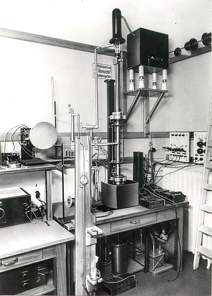
The electron microprobe, also known as the electron probe microanalyzer, developed utilizing two technologies: electron microscopy — the use of a focused high energy electron beam to interact with a target material, and X-ray spectroscopy — identification of the photons resulting from electron beam interaction with the target, with the energy/wavelength of the photons being characteristic of the atoms excited by the incident electrons. The names of Ernst Ruska and Max Knoll are associated with the first prototype electron microscope in 1931. The name of Henry Moseley is associated with the discovery of the direct relationship between the wavelength of X-rays and the identity of the atom from which it originated[6].

There have been at several historical threads to electron beam microanalytical technique. One was developed by James Hillier and Richard Baker at RCA. In the early 1940s, they built an electron microprobe, combining an electron microscope and an energy loss spectrometer.[7] A patent application was filed in 1944. Electron energy loss spectroscopy is very good for light element analysis and they obtained spectra of C-Kα, N-Kα and O-Kα radiation. In 1947, Hiller patented the idea of using an electron beam to produce analytical X-rays, but never constructed a working model. His design proposed using Bragg diffraction from a flat crystal to select specific X-ray wavelengths and a photographic plate as a detector. However, RCA had no interest in pursuing commercialization of this invention.

A second thread developed in France in the late 1940s. In 1948–1950, Raimond Castaing, supervised by André Guinier, built the first electron “microsonde électronique” (electron microprobe) at ONERA. This microprobe produced an electron beam diameter of 1-3 μm with a beam current of ~10 nanoamperes (nA) and used a Geiger counter to detect the X-rays produced from the sample. However, the Geiger counter could not distinguish X-rays produced from specific elements and in 1950, Castaing added a quartz crystal between the sample and the detector to permit wavelength discrimination. He also added an optical microscope to view the point of beam impact. The resulting microprobe was described in Castaing’s 1951 PhD Thesis,[8], translated into English by Pol Duwez and David Wittry [9], in which he laid the foundations of the theory and application of quantitative analysis by electron microprobe, establishing the theoretical framework for the matrix corrections of absorption and fluorescence effects. Castaing (1921-1999) is considered the “father” of electron microprobe analysis.

The 1950s was a decade of great interest in electron beam X-ray microanalysis, following Castaing’s presentations at the First European Microscopy Conference in Delft in 1949[10] and then at the National Bureau of Standards conference on Electron Physics[11] in Washington, DC, in 1951, as well as at other conferences in the early to mid-1950s. Many researchers, mainly material scientists, began to develop their own experimental electron microprobes, sometimes starting from scratch, but many times utilizing surplus electron microscopes.

One of the organizers of the Delft 1949 Electron Microscopy conference was Vernon Ellis Cosslett at the Cavendish Laboratory at Cambridge University, a center of research on electron microscopy[12], as well as scanning electron microscopy with Charles Oatley as well as X-ray microscopy with Bill Nixon. Peter Duncumb combined all three technologies and developed a scanning electron X-ray microanalyzer as his PhD thesis project (published 1957), which was commercialized as the Cambridge MicroScan instrument.

Pol Duwez, a Belgian material scientist who fled the Nazis and settled at the California Institute of Technology and collaborated with Jesse DuMond, encountered André Guinier on a train in Europe in 1952, where he learned of Castaing’s new instrument and the suggestion that CalTech build a similar instrument. David Wittry was hired to build such an instrument as his PhD thesis, which he completed in 1957. It became the prototype for the ARL[13] EMX electron microprobe.

During the late 1950s and early 1960s there were over a dozen other laboratories in North America, the United Kingdom, Europe, Japan and the USSR developing electron beam X-ray microanalyzers.

The first commercial electron microprobe, the “MS85” was produced by CAMECA (France) in 1956. It was soon followed in the early-mid 1960s by many microprobes from other companies. In addition, many researchers build electron microprobes in their labs. Significant subsequent improvements and modifications to microprobes included scanning the electron beam to make X-ray maps (1960), the addition of solid state Si(Li) LN2-cooled detectors (1968) and the development of synthetic multilayer diffracting crystals for analysis of light elements (1984).

Since the late-1990’s, a newer EDS detector – called the silicon drift detector (SDD) – has superseded the Si(Li) detector systems. The SDD consists of a high-resistivity silicon chip where electrons are driven to a small collecting anode. The advantage lies in the extremely low capacitance of this anode, thereby utilizing shorter processing times and allowing very high throughput. Benefits of the SDD include:

  • High count rates and processing,
  • Better resolution than traditional Si(Li) detectors at high count rates,
  • Lower dead time (time spent on processing X-ray event),
  • Faster analytical capabilities and more precise X-ray maps or particle data collected in seconds,
  • Ability to be stored and operated at relatively high temperatures, eliminating the need for liquid nitrogen cooling.

Because the capacitance of the SDD chip is independent of the active area of the detector, much larger SDD chips can be utilized (50 mm2 or more). This allows for even higher count rate collection. Further benefits of large area chips include:

  • Minimizing SEM beam current allowing for optimization of imaging under analytical conditions,
  • Reduced sample damage and
  • Smaller beam interaction and improved spatial resolution for high speed maps.

Applications

EDXRF spectrometers are the elemental analysis tool of choice, for many applications, in that they are smaller, simpler in design and cost less to operate than other technologies like inductively coupled plasma optical emission spectroscopy (ICP-OES) and atomic absorption (AA) or atomic fluorescence (AF) spectroscopy. Examples of some common EDXRF applications are:

Semiconductor and data storage

Biology and life sciences

Materials research

Industry

Don’t find the answer
yet?

Contact us and our team will reach out to you as soon as we can

  • This field is for validation purposes and should be left unchanged.