Micro X-ray Fluorescence for Thin-film Thickness & Composition

ATLAS SEMI microEDXRF Metrology Tool

ATLAS SEMI
Semi Software

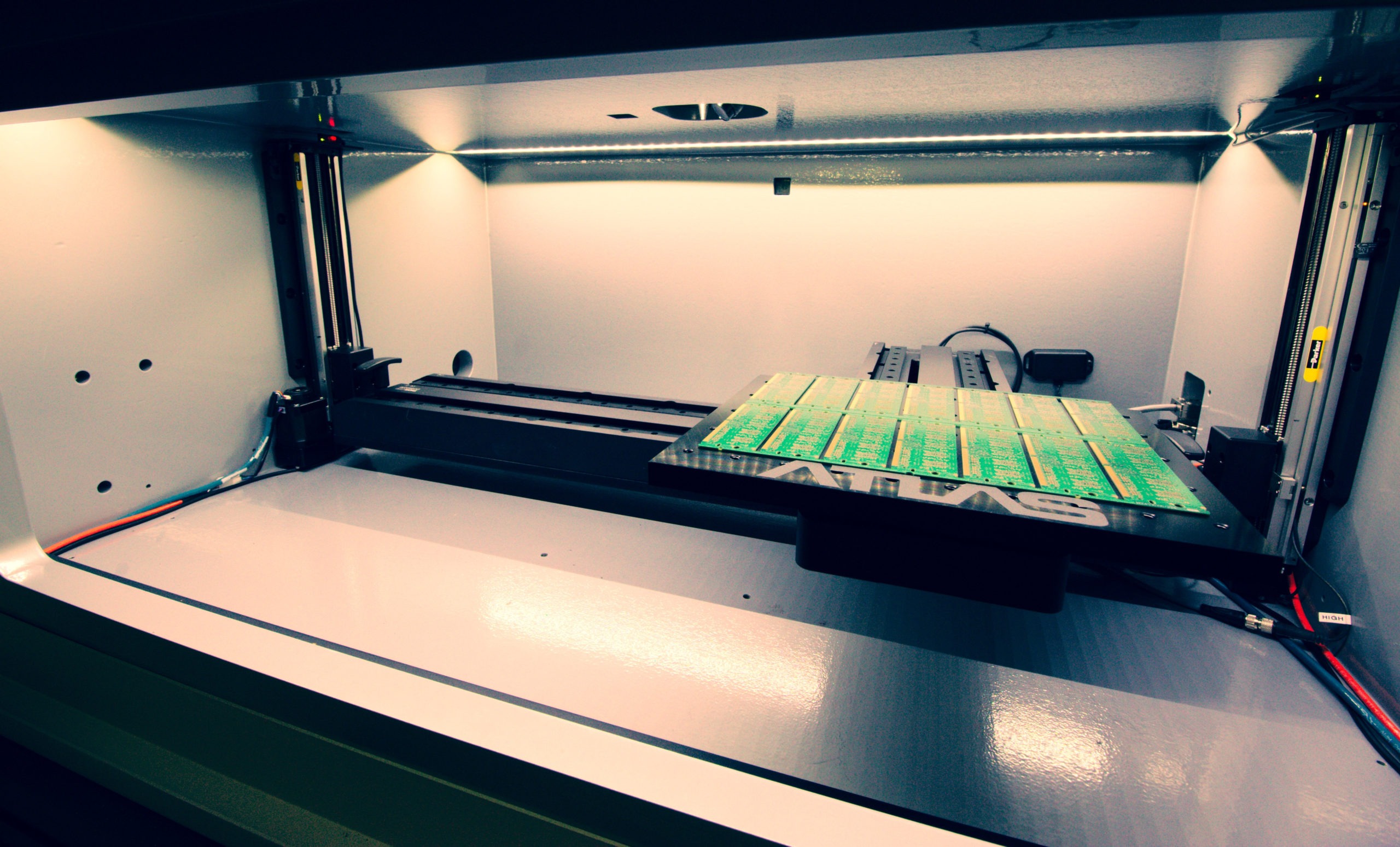
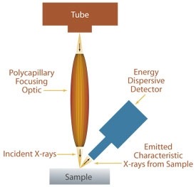
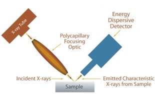
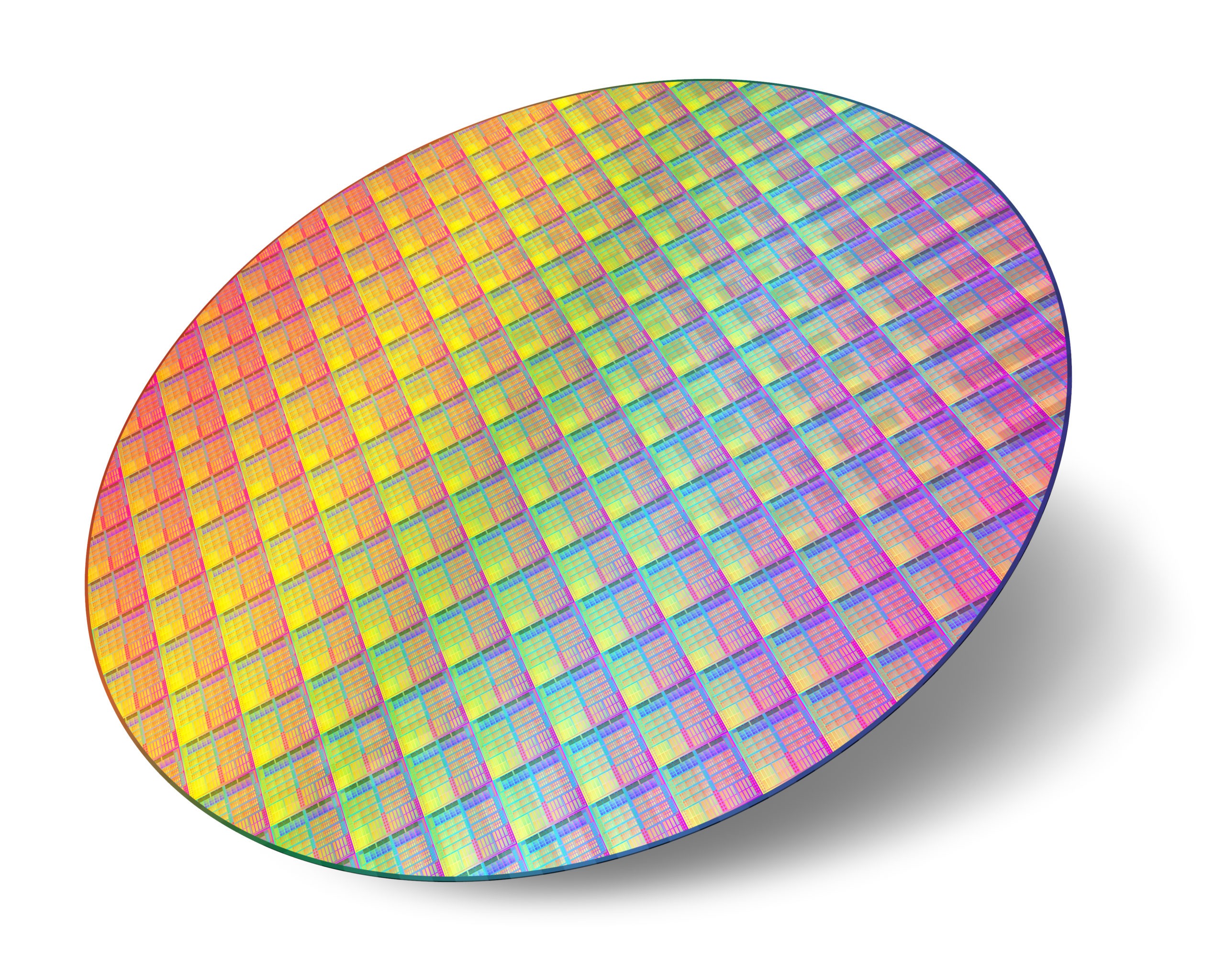
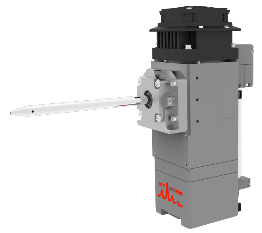
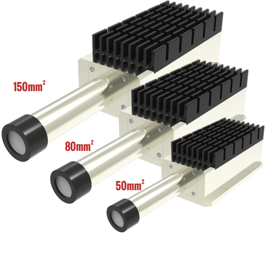
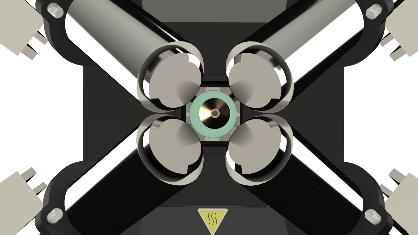
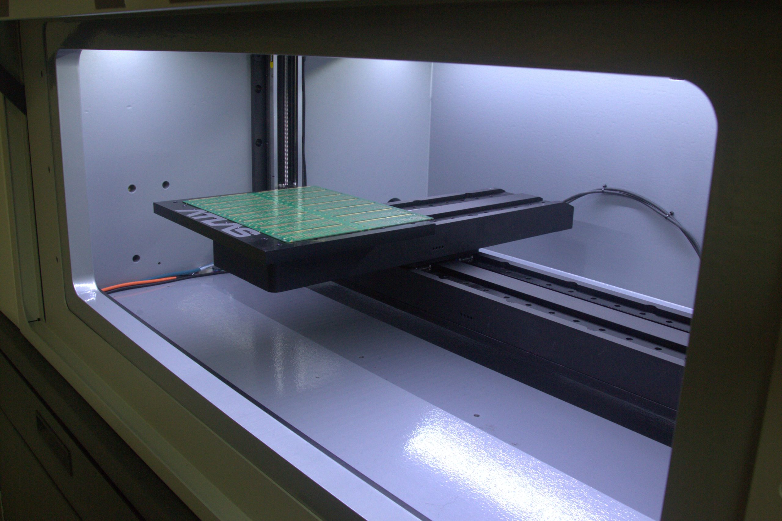
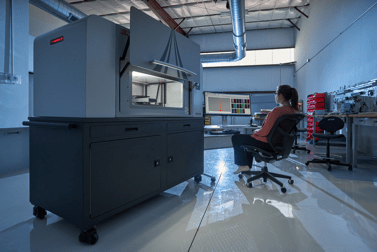
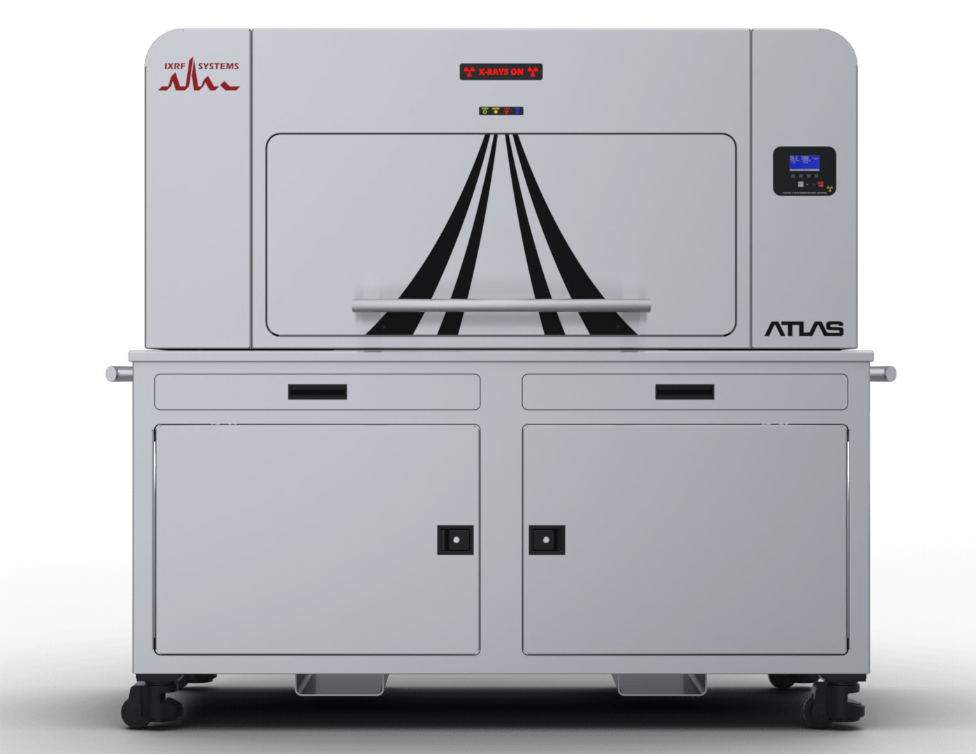
IXRF Systems’ ATLAS SEMI is the very latest micro spot energy dispersive X-ray fluorescence (micro XRF) imaging spectrometer for semiconductor metrology. Designed to image and analyze (edge-to-edge) wafers up to 300 mm diameter, ATLAS leads the industry in virtually every major specification category from the largest chamber and the highest detector active area, to the longest mapping travel and smallest X-ray micro-spot.

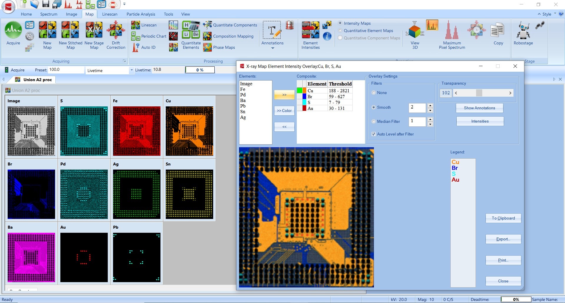
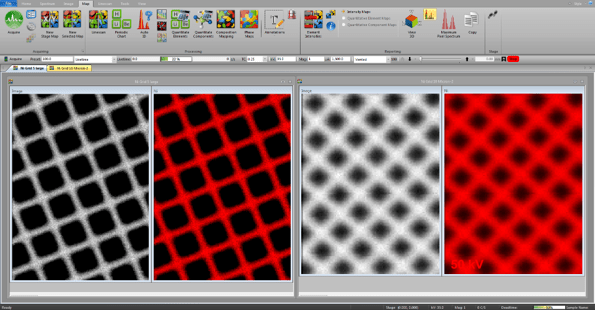
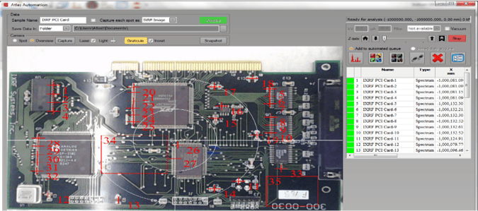
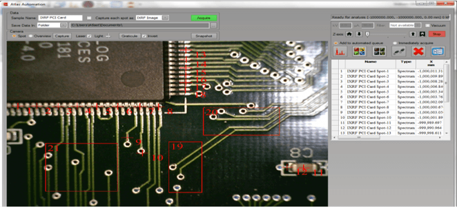
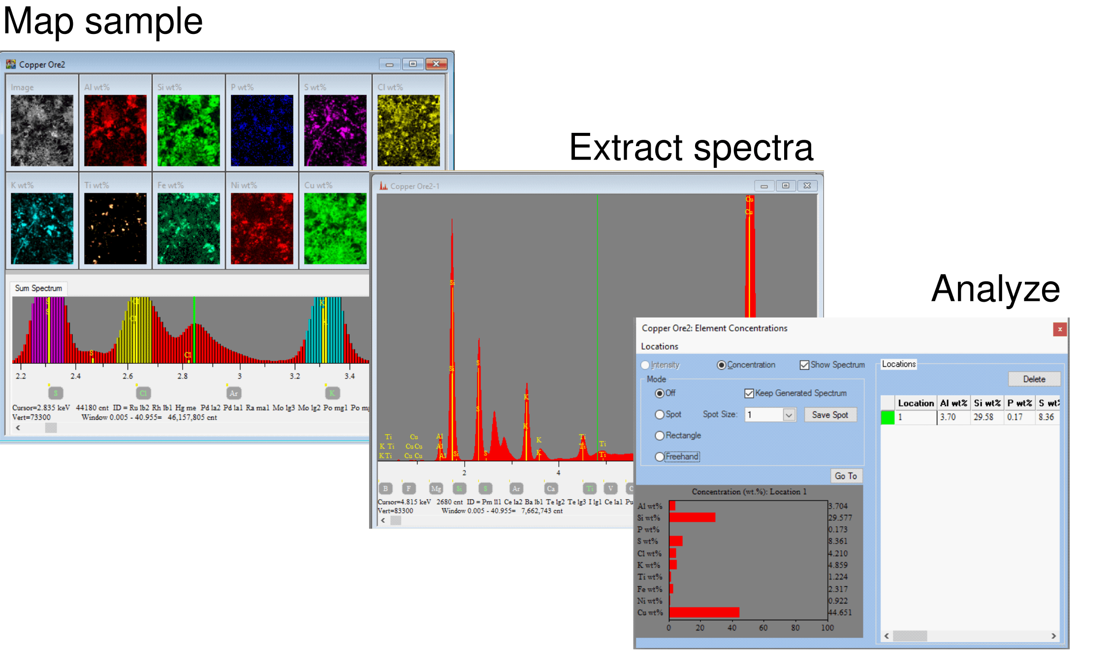
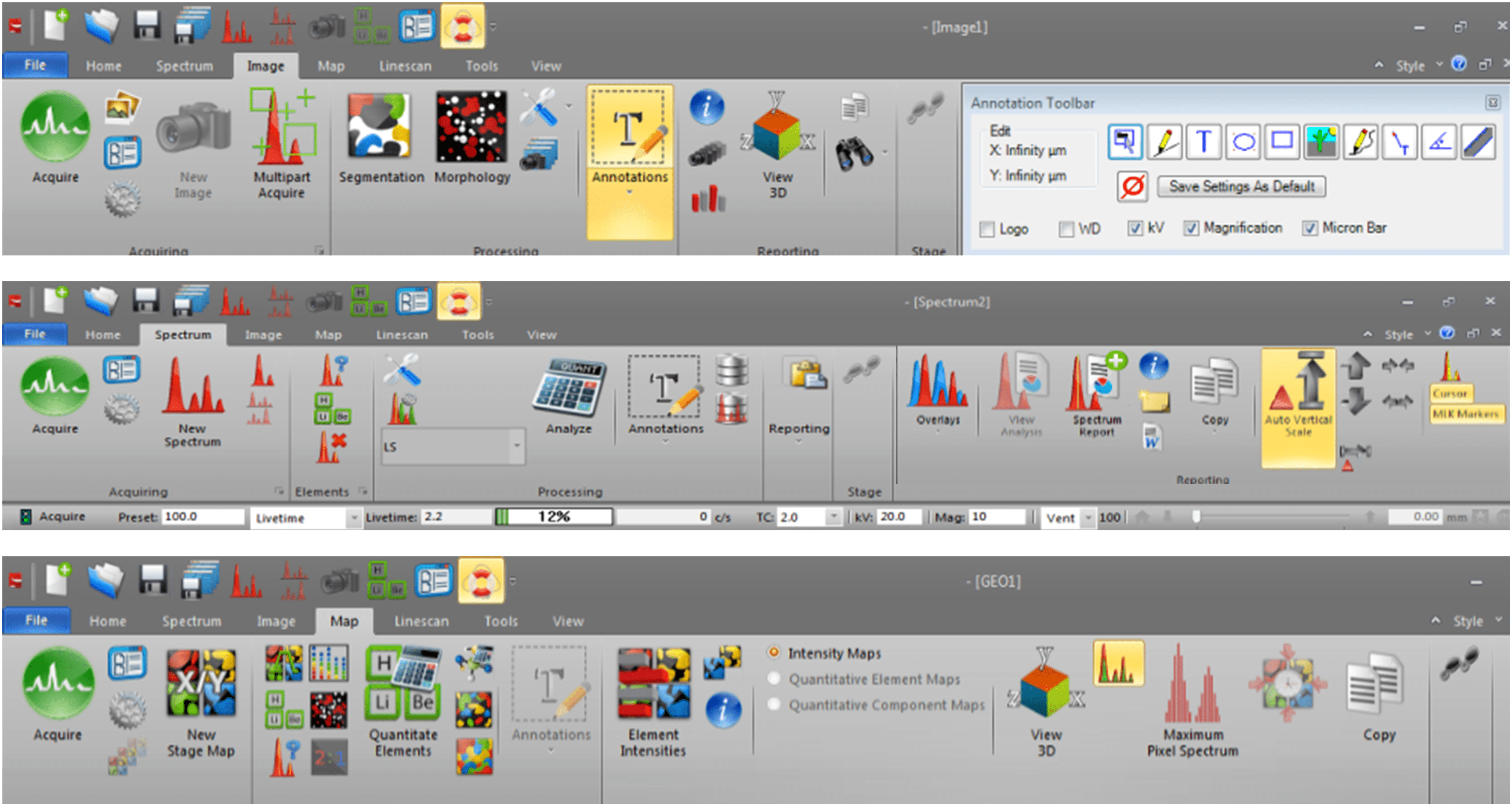
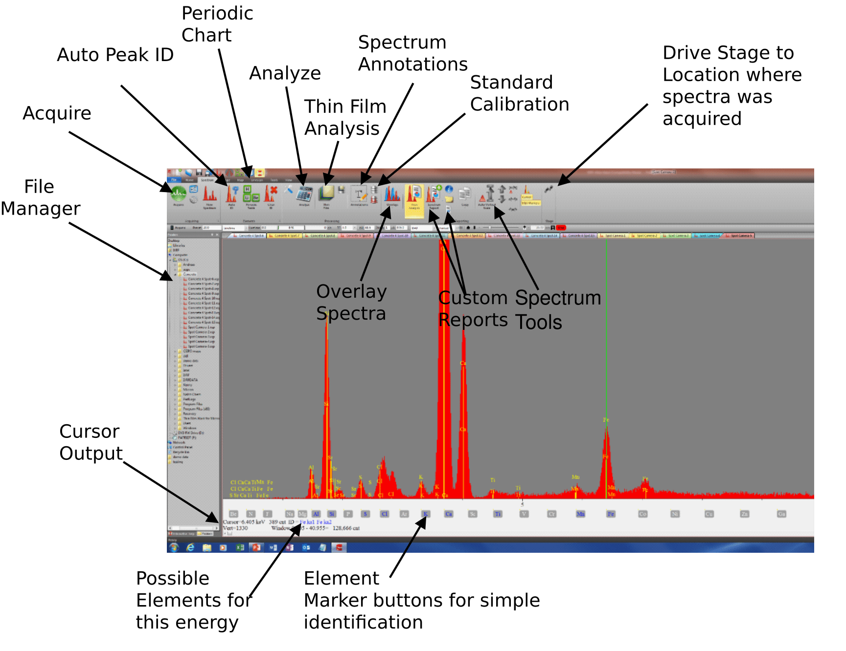
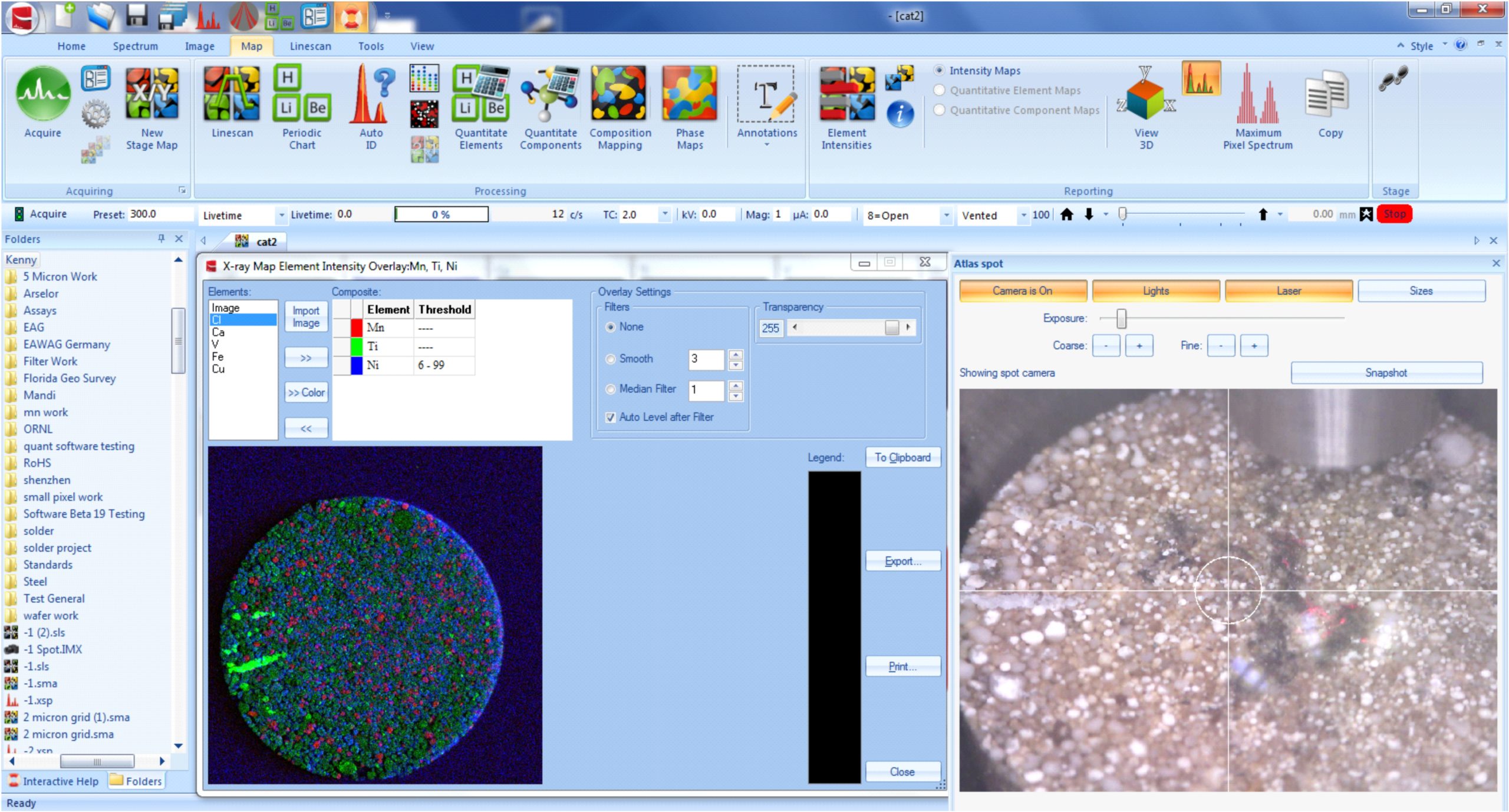
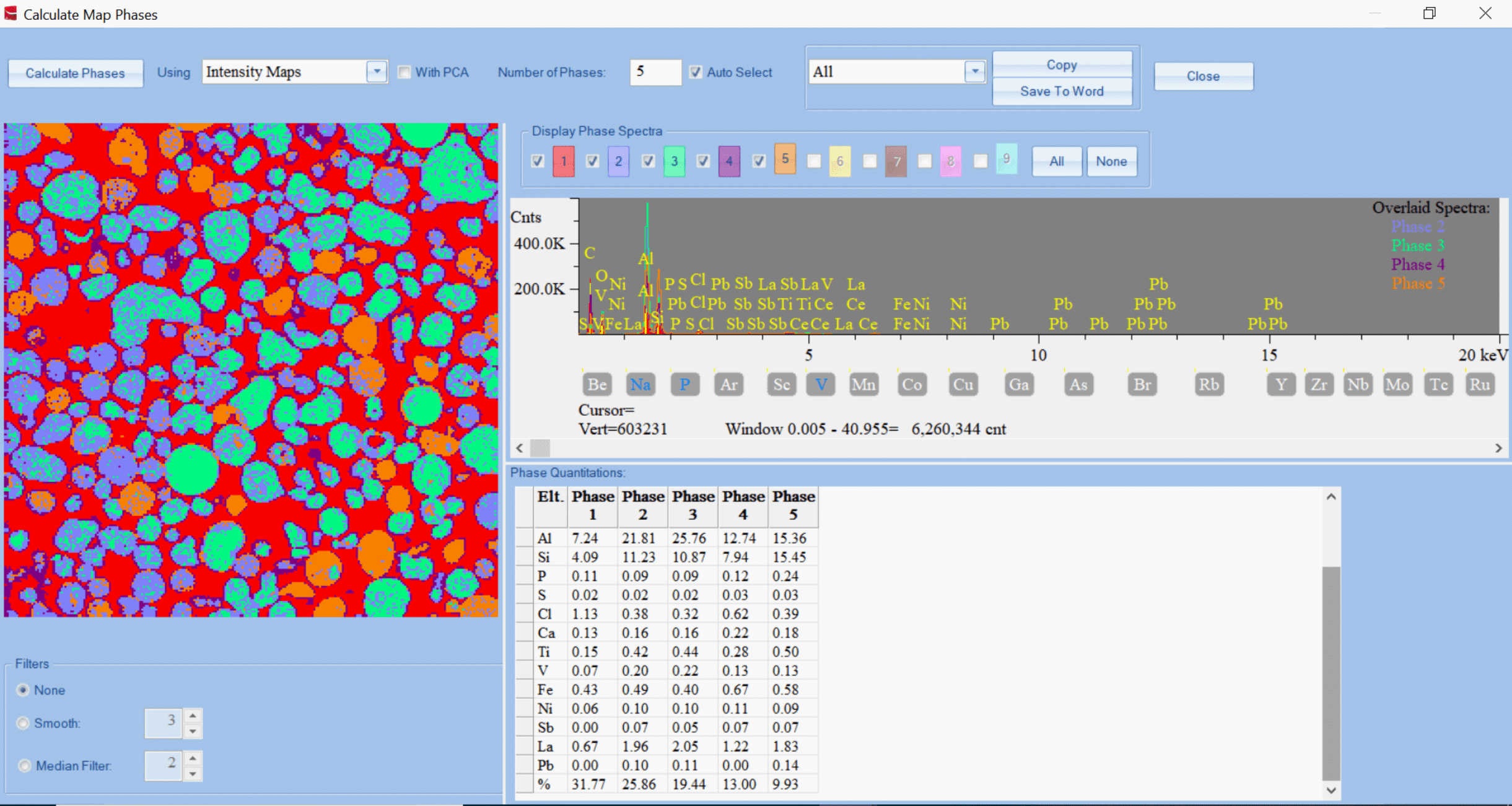
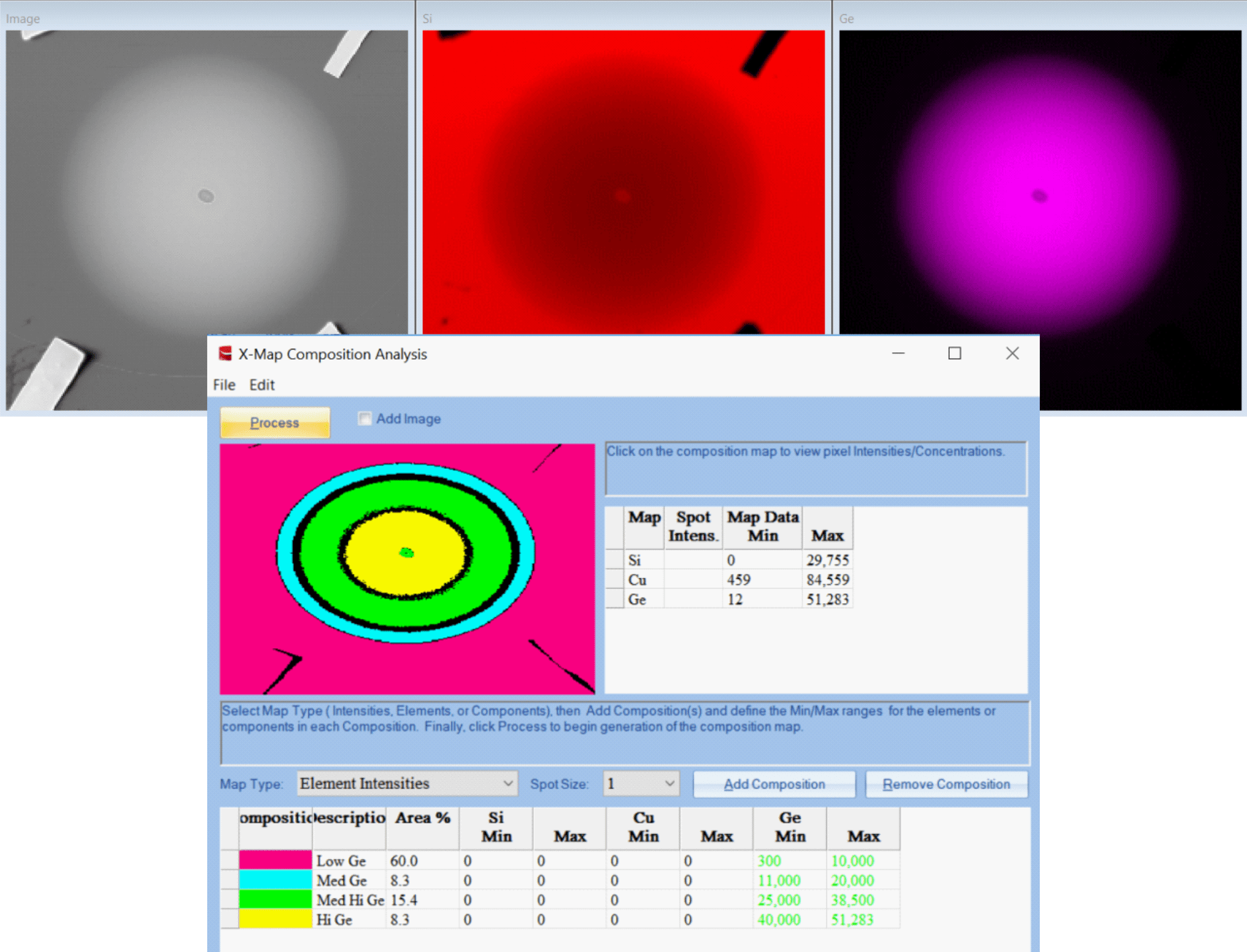
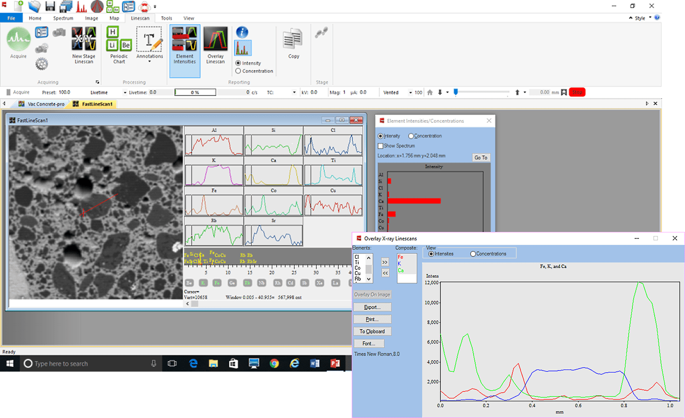
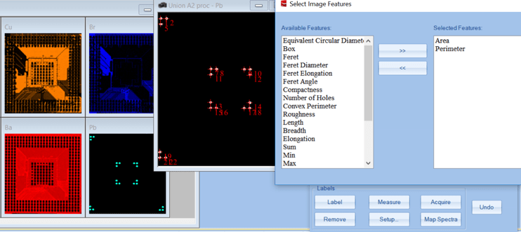
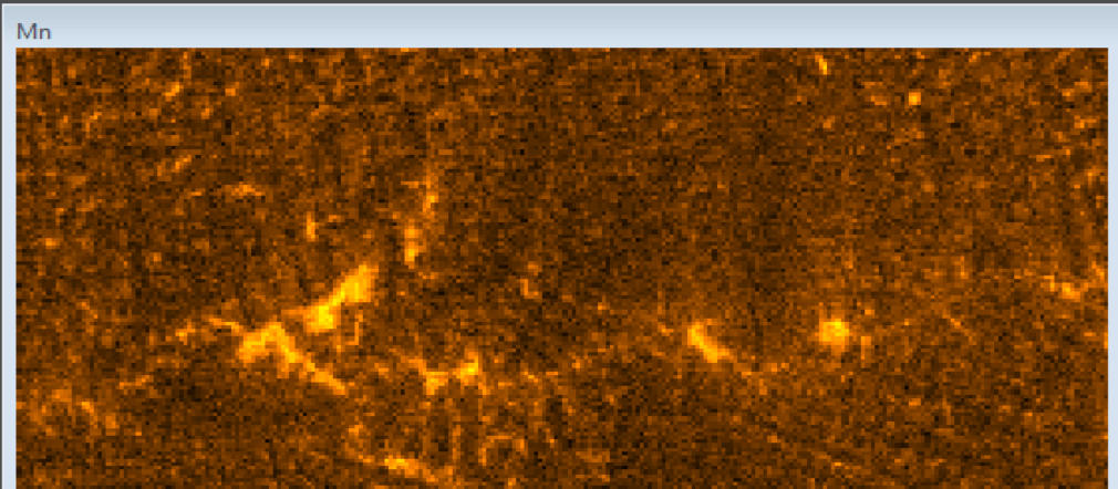
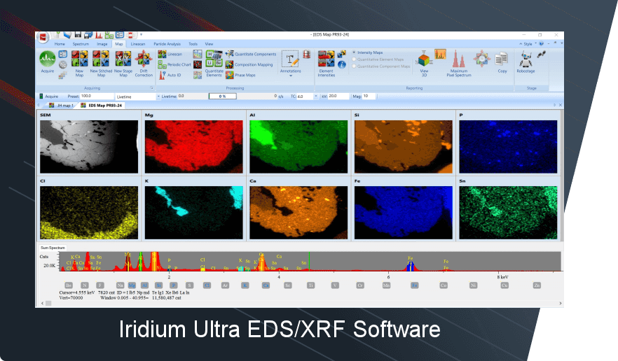
Hardware specifications are only half of the ATLAS Advantage™. ATLAS’ Iridium Ultra software platform, developed with SEM-EDS elemental mapping and analytical functionality, is unsurpassed in it’s ability to provide elemental and phase mapping, line scans, critical dimensions (CD) as well as qualitative and quantitative elemental analyses of multi-layer thin film stacks. The functional, flexible, and feature-rich software suite guarantees unprecedented productivity. ATLAS SEMI is the micro XRF metrology tool that leads with innovation.

download a brochure

Made in USAMicro X-ray fluorescence (µXRF, µEDXRF, micro-XRF, microEDXRF) spectroscopy is an elemental analysis technique that relies on the same principles as X-ray fluorescence (XRF) spectrometry. The difference is that micro x-ray fluorescence (microEDXRF) spectrometry has a spatial resolution with a diameter many orders of magnitude smaller than conventional XRF, WDXRF or EDXRF spectrometers. Practically, microEDXRF spectrometers with high-precision scanning XYZ-stages  — like the ATLAS series —  function as a type of  XRF hyperspectral imaging microscope, where each pixel (in a map or image) contains information from 4 – 40 keV in the electromagnetic spectrum.

Elemental Map Overlays
Atlas Logo

Modern polycapillary focusing X-ray optics are able to create small focal spots of just a few micrometers in diameter. By using such X-ray optics, the IXRF Systems’ ATLAS series of imaging spectrometers provide a tiny focal spot (down to  5 μm, depending on desired configuration) that is much more intense and allows for enhanced trace element analysis and the creation of hyperspectral images of a sample. Micro X-ray fluorescence (μEDXRF) spectometry is commonly employed in many applications, such as: botany, cement, forensics, small feature evaluations, elemental mapping, mineralogy, metals & alloys, electronics, multi-layered coating analysis, micro-contamination detection, film and plating thickness, biology and environment.*

Atlas X 10mm Lens

Biggest chamber

ATLAS SEMI micro-XRF imaging spectrometer features the industry’s most voluminous sample chamber, allowing for automation of more samples, larger area mapping capabilities, and wider variability of sample types that can be analyzed. Sample chamber size: 940 x 660 x 355 mm (37 x 26 x 14 inches).

The 5 micron advantage

ATLAS  SEMI micro-XRF mapping spectrometer is the FAB-LAB tool of choice for sample characterization using micro-X-ray spot energy dispersive X-ray fluorescence (microEDXRF) spectrometry for metrology information on composition (phase) and elemental distribution of multi-layer thin film stacks. With the smallest X-ray spot in the industry at 5 microns, ATLAS SEMI is optimized for analysis speed without compromising accuracy. The instrument can measure a wide range of sample types, whether small or large, even or irregularly shaped. Equipped with a large high-speed stage, it supports 2D analysis of virtually any kind of sample: small to 12 inch wafers, lead frames, circuit boards, bump bond pads, magnetic media, sputtering targets, etc. Its extra large vacuum chamber delivers superior light element (low-Z) sensitivity.

5um vs 10um spot size

When it comes to micro-X-ray microscopic imaging (mapping), smaller is always better. Above is a TEM grid. The image on the left was captured using the ATLAS SEMI's 5 micron X-ray spot. The inferior image on the right was taken with a 10 micron X-ray spot.

ATLAS geometry

ATLAS X w/ 5 µm round spot

conventional uEDXRF

Conventional w/ 25 µm oval spot

Superior geometry

  • Perpendicular ATLAS SEMI geometry allows for circular X-ray excitation down to 5 microns for highest spatial resolution.
  • Smallest spot means it is easier to find a flat aspect of a feature to measure.
  • Competitor’s inferior angled geometry only allows smallest spot to be 25 microns due to the ellipse.

Unmatched speed

  • Mix and match up to 4 Silicon Drift Detectors (SDD)
    • For the largest possible solid angle collection efficiency
  • Up to 600 mm2 active area
    • Available resolutions: ≤130-145 eV resolution
  • Highest count rate with the smallest spot for fast high-res images
Optical kernel

Overview automation

overview automation

Overview video camera mode:

  • Automated spectral spot analysis
  • Automated X-Ray mapping
  • Automated linescans
  • Large chamber view for large samples

Spot automation

spot automation

Video microscope mode:

  • 10 -200X magnification with auto zoom
  • Auto spectral  spot analysis
  • Automated X-ray mapping
  • Automated linescans

Intuitive software

Beginner users will find the software simple to navigate in a comprehensive manner. As they advance, more powerful tools are easily accessible with no additional cost. They are all included and not added on as options:

  • Custom report generation
  • Phase analysis
  • Particle analysis
  • Morphology
  • And ASTM testing methods
menu 1
menu 2
menu 3
Semi Wafer

Sample types and conditions

  • Air, vacuum or helium atmosphere
  • Vacuum ready in under one minute
  • Measure: patterned wafers (multi-layer thin films), circuit boards, lead frames, bond pads, magnetic media, sputtering targets … and we can measure liquids, particles and powders too.

Suggested Products

ATLAS SEMISEM-XRF Systems
Interested in what we do?

CONTACT US

  • Hi, my name is
  • and I am interested
  • in the
  • Please contact me at
  • or call me at
  • This field is for validation purposes and should be left unchanged.